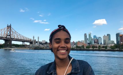
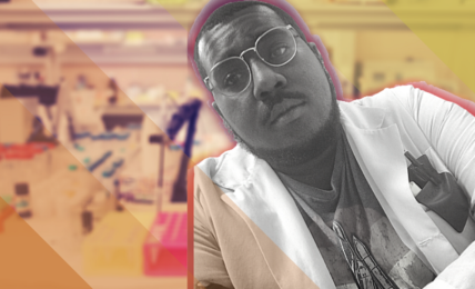
PROFILE: Daisy Shearer, experimental quantum physics PhD candidate
Read more about Daisy Shearer, a second-year Ph.D. candidate at the University of Surrey, U.K.

Read more about Daisy Shearer, a second-year Ph.D. candidate at the University of Surrey, U.K.
My name is Daisy Shearer, and I’m a second-year PhD candidate at the University of Surrey, U.K., where I work within the Photonics and Quantum Sciences Group at the Advanced Technology Institute. I also attended the University of Surrey for my undergraduate integrated Masters (MPhys) degree, where I studied physics for four years, including one year doing research in an industry setting for my master’s dissertation. I was placed at the Centre for Integrated Photonics where I had the amazing opportunity to do R&D on electroabsorption modulated lasers for long-haul telecommunications applications. This research experience gave me a taste for experimental quantum physics, and I haven’t really looked back since!

My doctoral research sits in the realm of quantum technology—a field that combines fundamental physics with materials science and has the overall aim of making new technological advances which utilise quantum mechanical phenomena. The most well-known of these potential technologies is probably quantum computing.
I focus on a type of material called semiconductors, specifically those which are made up of a combination of elements from groups 3 and 5 of the periodic table which we call ‘III-V semiconductors’. These types of materials are commonly found in electronic devices that use transistors such as computers and smartphones.

Whereas our current technologies primarily use electronics to function, my research is in the area of ‘semiconductor spintronics (spin transport electronics)’. Essentially I’m using semiconductor materials to find ways to control both the electrical current and the spin state of electrons in these materials. This gives spintronics devices additional degrees of freedom and the potential to store a lot more information in one electron than is possible with conventional electronics.
The main aim of my doctoral project is to investigate ways in which we can produce a ‘spin-polarized current’ in indium antimonide based semiconductor nanostructures. Spin-polarized current is a flow of electrons that has one particular spin state. This current can then be used to ‘inject’ electrons of a known spin state into a quantum technology device. For example, electron spin qubits used in quantum computers need to first be initialized to a certain known spin state before a quantum operation can be performed. Because of the quantum mechanical nature of the systems I work with, producing said spin-polarized current is easier said than done. It requires both a deep understanding of the quantum mechanics of solid-state physics as well as the ability to fabricate devices made from semiconductor materials.
Day-to-day, my research involves a combination of device fabrication, like using a Focused Ion Beam to etch nano constrictions called ‘quantum point contacts’ from semiconductor heterostructures, experimental testing, like using a superconducting magnet to investigate how magnetic fields interact with the device via mechanisms such as the quantum Hall effect and computational simulations to inform and validate experimental work.

I was diagnosed with autism spectrum disorder towards the end of my degree in 2017 at the age of 21. Since diagnosis, I have come to accept myself for who I am as well as learning ways to better navigate the challenges that come along with being autistic. Because of this, as well as a passion for science communication, I started sharing snapshots of my ‘PhD journey’ on social media a few months into my PhD program.
I enjoy sharing my work and thoughts on my Instagram page (@notesfromthephysicslab) so much that I have expanded my online presence into a blog and the occasional YouTube video to explore different formats and lengths of communication.
As well as exploring physics concepts related to my research, I use my online presence to talk about my personal experiences as an autistic person as well as a woman in physics. My hope is that by opening up discussions around these topics and sharing what I learn along the way, I can raise some awareness around being an autistic adult and maybe help others like me feel like they belong in STEM.
I’m particularly passionate about making STEM more accessible and inclusive for neurominorities as well as disabled people more generally. I run a project called ‘Neurodivergent in STEM’ which shares the stories of a wide range of neurodivergent people in STEM fields (i.e., those of us with conditions like autism, ADHD, dyslexia, and dyspraxia) to show the world that we are incredibly diverse. We hope that by sharing our experiences, we can move towards a more supportive and inclusive environment for us within STEM.
Connect with Daisy:
All images courtesy of Daisy Shearer.